MSXB 044 Signal Conditioning Board
Technical Note TN-229 Version 1.10
The Microstar Laboratories Signal Conditioning Board, part number MSXB 044, provides analog input signal conditioning for the iDSC 1816. Each Signal Conditioning Board provides analog input signal conditioning for two analog input channels. The Signal Conditioning Board is compatible with the MSXB 047 Signal Conditioning Backplane.
The Signal Conditioning Board provides AC/DC coupling, programmable gain, and DC voltage offset for each input channel. Each of these features is programmable on a channel-by-channel basis so that many different combinations of sensors can be used.
Each channel has a voltage source for sensors that require voltage excitation. DC excitation voltage levels are individually programmable. A 4mA current source is also included for each channel for sensors that require current excitation, such as ICP-type and Isotron-type accelerometers.
The Signal Conditioning Board must be used in conjunction with the MSXB 047 Signal Conditioning Backplane and the MSXB 046 Signal Conditioning Interface Board. Up to four Signal Conditioning Boards can be connected to the MSXB 047 backplane for a total of eight input channels.
Installation
The Signal Conditioning Board connects directly to the MSXB 047 Signal Conditioning Backplane via connector J1. The Signal Conditioning Board can be installed into slot J2, J3, J4, or J5 of the MSXB 047 backplane. The slot the Signal Conditioning Board is installed in is used to select which two channels on the iDSC 1816 the Signal Conditioning Board is mapped to. Table 1 below shows which slots on the MSXB 047 backplane are mapped to which channels on the iDSC 1816.
| Table 1. MSXB 047 Channel Map | |
|---|---|
| MSXB 047 slot | IDSC 1816 channels |
| J2 | A0, A1 |
| J3 | A2, A3 |
| J4 | A4, A5 |
| J5 | A6, A7 |
The MSXB 046 interface board must be installed into the slot J1 of the MSXB 047 backplane. The MSXB 046 provides the interface to the iDSC 1816 as well as power for the MSXB 047 and MSXB 044 boards. J2 of the MSXB 046 is connected to the iDSC 1816 using a MSCBL048 or MSCBL050.
When installing a board into the backplane, push the board firmly into the slot and make sure the board is securely connected to the backplane. Next, secure the front panel of the board to the enclosure with the two screws.
Warning: Never install a board into the backplane or remove a board from the backplane while the backplane is powered.
The MSXB 046 is powered externally via an 8-line mini-DIN connector, J3, on the front panel of the board. The MSXB 046 can be connected to a standard PC power supply by using both an MSCBL080-01 and an MSCBL081-02. The MSCBL081-02 installs inside the PC and is used to bring power out from the PC power supply to an 8-line mini-DIN panel mount connector on the back of the PC. The MSCBL080-01 is used to connect the MSXB 046 to the 8-line mini-DIN power connector on the back of the PC. The MSXB 046 typically requires 2.33 Amps at +12 Volts DC. The user should check and make sure that the total current drawn from the PC power supply does not exceed its limits.
Hardware Configuration
The following diagram shows the layout of the Signal Conditioning Board:
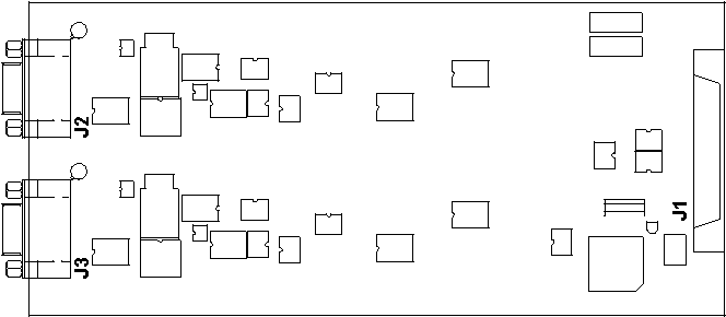
Figure 1. MSXB 044
The input signals come into the board through connectors J2 and J3. Connectors J2 and J3 are High Density DB-15 connectors which are located on the left side of the board in Figure 1 above. Each connector brings signals for one input channel into the board. J2 corresponds to the even channel and J3 corresponds to the odd channel on the iDSC 1816. The pin diagram for each connector is shown in Figure 2 below.
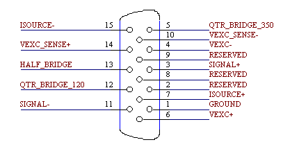
Figure 2. Input Connector Pin Diagram
Pin 1 is the signal ground.
Pin 2, pin 8 and pin 9 are reserved, and should not be connected.
Pin 3 (SIGNAL+) and pin 11 (SIGNAL-) are the voltage differential inputs.
Pin 7 (ISOURCE+) and pin 15 (ISOURCE-) are the current excitation source and its ground return. The current source is used for ICP accelerometers as shown in Figure 3 below:
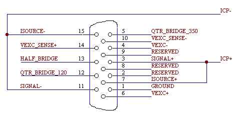
Figure 3. ICP accelerometer input
Pin 6 (VEXC+) and pin 4 (VEXC-) are the voltage excitation source and its ground return. Pin 14 (VEXC_SENSE+) and pin 10 (VEXC_SENSE-) are the voltage excitation sense inputs. VEXC_SENSE+ should be connected to VEXC+ at the sensor. Also, VEXC_SENSE- should be connected to VEXC- at the sensor. The voltage excitation source is used for strain gauges as shown in Figure 4 below:
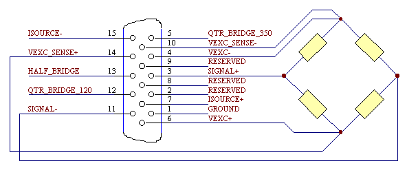
Figure 4. Strain gauge input
Pin 13 (HALF_BRIDGE) is used for half bridge completion as shown in Figure 5 below:
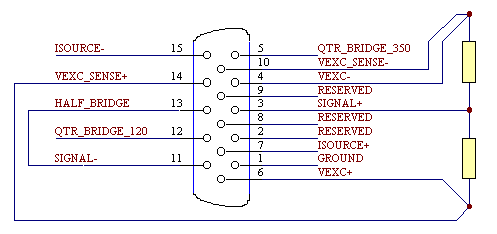
Figure 5. Half bridge completion
Pin 5 (QTR_BRIDGE_350) is the quarter bridge completion for a 350 Ohm quarter bridge strain gauge as shown in Figure 6 below:
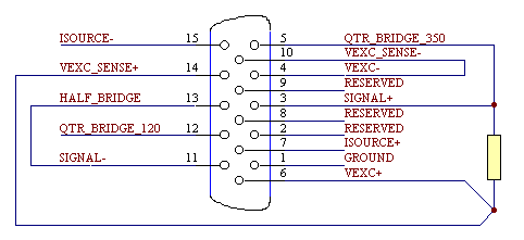
Figure 6. 350 Ohm quarter bridge completion
Pin 12 (QTR_BRIDGE_120) is the quarter bridge completion for 120 Ohm quarter bridge strain gauge as shown in Figure 7 below:
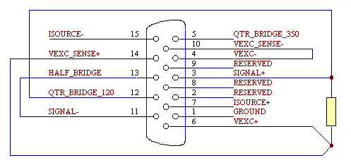
Figure 7. 120 Ohm quarter bridge completion
View other Technical Notes.