MSXB 037 Analog Input Expansion Board
Technical Note TN-186 Version 1.2
The Microstar Laboratories Analog Input Expansion Board, part number MSXB 037, provides analog input expansion for analog backplane systems. The Analog Input Expansion Board is compatible with the MSXB030-01 and MSXB031-01 Analog Backplanes.
The Analog Input Expansion Board provides 16 single-ended or eight differential analog inputs with on-board termination points. Up to 32 Analog Input Expansion Boards can be connected to a DAP for 512 inputs.
Several models of the MSXB 037 are available. The MSXB 037-01-E2C connects directly to the Analog Backplane. It has a 20-BNC end panel that takes the space of five backplane slots. The MSXB 037-01-E2Y also connects directly to the Analog Backplane. It ha s a blank end panel that takes the space of one backplane slot. The MSXB 037-01-A2Z is a stand-alone model that is used without an Analog Backplane. It connects directly to the Data Acquisition Processor by means of a cable.
Installation
The Analog Input Expansion Board connects directly to the analog backplane via connector J1. The Analog Input Expansion Board can be installed into any available slot in the analog backplane, as long as it has enough room for the end panel.
When installing the Analog Input Expansion Board, push the board firmly into the slot and make sure the board is securely connected to the backplane.
The stand-alone model connects to the Data Acquisition Processor by means of the MSCBL040-01 or the MSCBL041-01 68-line cable.
Warning: Never install a board into the backplane or remove a board from the backplane while the backplane is powered.
Hardware Configuration
The following diagram shows the layout of Analog Input Expansion Board:
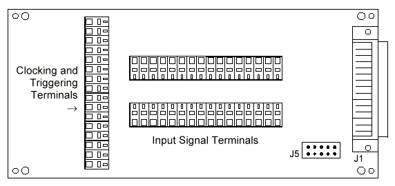
Figure 1. MSXB 037
The input signal terminals on the Analog Input Expansion Board are labeled S0, S1, etc. The input ground terminals are labeled G0, G1, etc.
Note: If the Data Acquisition Processor does not have fault-protected input multiplexers, signals must not be applied to the Analog Input Expansion Board when power is not applied to the Data Acquisition Processor.
The Analog Input Expansion Board is factory configured for voltage input. It also can be configured for current input or for input voltages that exceed Data Acquisition Processor specifications.
The Analog Input Expansion Board also has an area for building custom circuits. The terminals on the Analog Input Expansion Board accept wire sizes from 14 to 26 AWG.
The Analog Input Expansion Board also can be used for differential inputs. A differential input is used to measure the difference between two voltages. The negative terminal voltage is subtracted from the positive terminal voltage. When a differential voltage is measured, a ground sense line must be connected between the Analog Input Expansion Board and the signal source. Table 1 shows the correspondence between differential and single-ended inputs.
Single-Ended Input      Differential Input
       S0                      D0-
       S1                      D0+
       S2                      D1-
       S3                      D1+
       S4                      D2-
       S5                      D2+
       S6                      D3-
       S7                      D3+
       S8                      D4-
       S9                      D4+
       S10                     D5-
       S11                     D5+
       S12                     D6-
       S13                     D6+
       S14                     D7-
       S15                     D7+
|
Input Range Selection
Up to 32 Analog Input Expansion Boards can be connected to a DAP for 512 inputs. The Analog Input Expansion Board must be configured to recognize a specific input address range. The jumper setting on connector J5 selects this range.
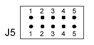
Pin 1 of connector J5 is closest to the middle of the board. The input range is selected according to the following table:
Input Range Jumper Setting 0 - S15 1, 2, 3, 4, 5 S16 - S31 1, 2, 3, 4 S32 - S47 1, 2, 3, 5 S48 - S63 1, 2, 3 S64 - S79 1, 2, 4, 5 S80 - S95 1, 2, 4 S96 - S111 1, 2, 5 S112 - S127 1, 2 S128 - S143 1, 3, 4, 5 S144 - S159 1, 3, 4 S160 - S175 1, 3, 5 S176 - S191 1, 3 S192 - S207 1, 4, 5 S208 - S223 1, 4 S224 - S239 1, 5 S240 - S255 1 |
Input Range Jumper Setting S256 - S271 2, 3, 4, 5 S272 - S287 2, 3, 4 S288 - S303 2, 3, 5 S304 - S319 2, 3 S320 - S335 2, 4, 5 S336 - S351 2, 4 S352 - S367 2, 5 S368 - S383 2 S384 - S399 3, 4, 5 S400 - S415 3, 4 S416 - S431 3, 5 S432 - S447 3 S448 - S463 4, 5 S464 - S479 4 S480 - S495 5 S496 - S511 none |
Each jumper setting on connector J5 selects an address range of 16 input channels. When using multiple Analog Input Expansion boards, each board must be configured with a unique address range.
Analog Output Connections
The two Data Acquisition Processor digital-to-analog converter outputs are available on the Analog Input Expansion Board, labeled DAC0 and DAC1. Each has an associated ground return, labeled DAC0G and DAC1G.
The output current from each digital-to-analog converter output is rated at +/-5 milliamps; however, Microstar Laboratories recommends that this current not exceed +/-1 milliamp. The digital-to-analog converter outputs are voltage outputs.
Clocking and Triggering Connections
Clocking and triggering signals can be connected to the Analog Input Expansion Board. See the Data Acquisition Processor manual for more information about hardware clocking and triggering.
External clock and trigger signals connected to the Analog Input Expansion Board must be in the standard TTL range of 0 to 5 volts.
The clocking and triggering labels on the Analog Input Expansion Board are defined as follows:
IXCIN= External Input Clock - InputIXTIN= External Input Trigger - InputINCLK= Internal Input Clock - OutputOXCIN= External Output Clock - InputOXTIN= External Output Trigger - InputOUTCLK= Internal Output Clock - Output
Current Input Configuration
To configure the Analog Input Expansion Board for a current input, place a resistor in the location on the board corresponding to the input pin being reconfigured. Figure 3 and Table 3 show resistor placement. The appropriate size for this resistor can be calculated using Ohm's Law, given the maximum input current and the input voltage range of the Data Acquisition Processor.
Ohm's Law: Resistance = Voltage / Current
The Data Acquisition Processor is shipped from the factory with an input range of +/-5 volts. The accuracy of the measurements made in this configuration depends on the precision of the resistors used, which should be taken into consideration when selecting the resistors. Microstar Laboratories recommends using resistors with a 1% or better tolerance.
Excess power dissipated in the resistor causes heating which changes the resistance value and decreases the accuracy of the measurements. The recommended maximum power dissipation is 0.1 Watt.
Power Calculation: Power = current2 * resistance
For current input, a current source is connected to the Sx terminal and the ground return is connected to the Gx terminal. To convert voltage input S0 into a current input that generates 1 to 5 volts with an input current of 4 to 20 milliamps, a 250 ohm resistor is inserted in the R1 location. In this case, the maximum power dissipated in the resistor is 0.1 watt at +5 volts; this is the maximum recommended power dissipation. Figure 2 illustrates the connections for this example.
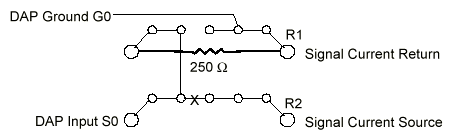
Figure 2. Resistor Connection for Current Input
Voltage Divider Configuration
Warning: Be careful to avoid applying an input voltage to the Data Acquisition Processor that exceeds specifications.
The Analog Input Expansion Board can be configured for applications requiring input voltages greater than that allowed by the Data Acquisition Processor. This is accomplished by soldering a resistive voltage divider in the locations provided on the board.
Before installing the voltage divider, a trace on the termination board must be cut. Above each even numbered resistor there is a row of five small holes. Between two of the holes there is a white "X." The trace must be cut at the "X."
Danger: If the trace on the termination board is not cut, the high-voltage input is connected directly to the Data Acquisition Processor input; this may destroy the Data Acquisition Processor.
Once the trace is cut, the resistors for the voltage divider are soldered into place. The resistor on the ground side of the divider is placed in an odd-numbered resistor location and the resistor on the input signal side of the divider is placed in an even-numbered resistor location. Figure 3 and Table 3 illustrate resistor placement for each input.
After both resistors are soldered into place, signals may be connected between the Sx and Gx terminals. Test the voltage divider circuit before connecting the circuit to the Data Acquisition Processor.
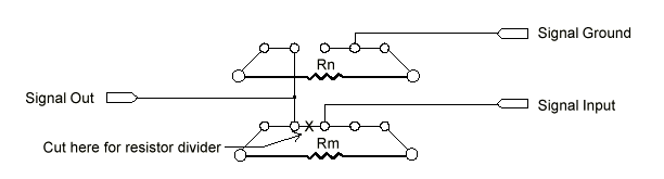
Figure 3. Resistor Placement
The following equation is used to calculate voltages and resistances:
Voltage Divider Equation: V out = V in * Rn/(Rn+Rm)
Note: To avoid exceeding Data Acquisition Processor input voltage specifications, make sure both resistors are securely soldered in the correct locations and the trace beneath the X is completely cut before using the circuit.
Terminal Current Input Resistor* Voltage Divider Resistors S0, G0 R1 R1, R2 S1, G1 R3 R3, R4 S2, G2 R5 R5, R6 S3, G3 R7 R7, R8 S4, G4 R9 R9, R10 S5, G5 R11 R11, R12 S6, G6 R13 R13, R14 S7, G7 R15 R15, R16 S8, G8 R17 R17, R18 S9, G9 R19 R19, R20 S10, G10 R21 R21, R22 S11, G11 R23 R23, R24 S12, G12 R25 R25, R26 S13, G13 R27 R27, R28 S14, G14 R29 R29, R30 S15, G15 R31 R31, R32 |
* The current input resistor is placed in the Rn location shown in Figure 3.
** The first resistor is on the ground side of the voltage divider (Rn), the second is on the input signal side (Rm), as shown in Figure 3. For example, R1 is Rn and R2 is Rm. Figure 4 shows the resistor placement for this example.
Table 3 and Figure 3 can be used to locate the appropriate resistors when using either the current input or voltage division configuration. Figure 3 shows schematically how the inputs and grounds on the termination board are connected.
Voltage Divider Example: To configure input S0 so that an input range of 0 to 20 volts is scaled down to a range of 0 to 5 volts, a resistor ratio of 3:1 is needed, as determined by the Voltage Divider Equation.
Resistance values of 1500 and 500 Ohms may be used. The trace beneath the X above R2 is cut. Then the 500 Ohm resistor is placed in the R1 position and the 1500 ohm resistor is placed in the R2 position. Since 500 Ohm resistors are not commonly available, a 510 Ohm resistor would typically be used instead, resulting in a small error in the division ratio. This error is linear and can be corrected by multiplying by a constant in DAPL. Figure 4 illustrates the circuit for this example.
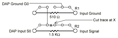
Figure 4. Resistor Circuit for S0
Cold Junction Reference
The Analog Input Expansion Board has a cold junction reference circuit to measure the temperature of the "cold junction" at the input termination on the Analog Input Expansion Board. Since the cold junction termerature is the same for all thermocouples connected to the Analog Input Expansion Board, only one cold junction reference circuit is needed for any number of thermocouples.
The cold junction circuit generates a voltage that is temperature dependent. The output of this circuit is connected to input S8 by means of jumper header J6. Installing both shunts on header J6 connects the cold junction circuit output to input S8. Removing both shunts on header J6 disconnects the cold junction circuit from S8 and allows the use of input S8.
Note: When the cold junction reference circuit is connected to S8, no other inputs may be connected to the S8 input terminal.
The cold junction reference circuit consists of a Linear Technology LT1025A integrated circuit. The LT1025A has a linear voltage output which is directly proportional to the temperature in degrees Celsius. The LT125A outputs 0V at 0 degrees Celsius and 10mV for every degree above zero. At 25 degrees Celsius, the LT1025A will output 250mV. The cold junction reference circuit will not operate at temperatures below 0 degrees Celsius or above 50 degrees Celsius.
Power Consumption
The Analog Input Expansion Board consumes power from the analog backplane through three voltage supplies: +5V, +18V, and -18V. The following table lists the maximum current drawn from each voltage supply under worst case conditions:
Power Supply    Current Drawn (mA)
    +18V              7.0
    -18V              6.5
    + 5V            100.0
|
When using multiple Analog Input Expansion Boards in a backplane, extreme caution must be used to avoid exceeding the current limits of the analog backplane. Please refer to the Analog Backplane documentation for information on power consumption.
The stand-alone model of the Analog Input Expansion Board draws power from the DAP's voltage supplies: +5V, +18V, and -18V. Extreme caution must be used to avoid exceeding the current limits of the DAP. Please refer to the DAP hardware documentation for information on its power availability.
The +18V and -18V supply voltages are available on the Analog Input Expansion Board termination connector. Extreme caution must be used to avoid exceeding the current limits of the system.
End Panel Connections
The backplane models of the Analog Input Expansion Board have two standard end panels: blank and BNC connectors. A blank end panel allows the user to create custom connection points. A BNC end panel provides direct connections to the Analog Input Expansion Board.
BNC End-Panel Connections
Each BNC connector can be wired to any termination point on the Analog Input Expansion Board. In the standard configuration, the BNC connectors map to the Analog Input Expansion Board as follows:
   S0-S15 ........... analog input channels S0-S15
   DAC0, DAC1 ....... not connected
   AG ............... not connected
   G ................ signal ground G0
All signal grounds should be connected to G.
View other Technical Notes.